
( Developed by José Francisco for his MSc thesis )
Eye trackers can provide valuable information about the user reactions or interest even in Virtual Reality Systems. In these cases, and especially when head mounted displays (HMD) are in use the solution is to install the image capture setup inside the HMD itself.
In this article you can find the description of the construction of a low cost solution for the Oculus Rift DK2.
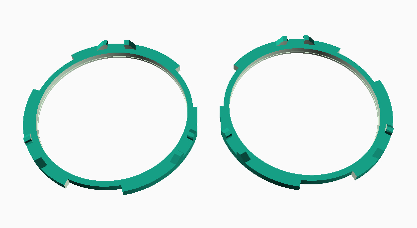
Spacer construction
To construct the spacer we start by 3D printing two different parts for each lens. They where based upon the "Parametric Rift DK2 IPD adjuster", published on "www.thingiverse.com" by "ClassicGOD" thingiverse, used for changing the inter pupilar distance of the lenses.
Bottom parts (Rendering)
[Links to files of the models]
Note that the left and right parts are mirrors of each other and that they have a flat edge on the axis of symmetry. This flat edge is necessary for the spacers to fit correctly on the HMD, and as such when both spacers are placed on the HMD the left and right one should face each other.
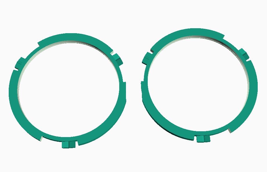
Assembling the pieces together
After printing, a small modification needs to be done on the bottom parts. Part of the piece needs to be cut off in order for the camera to fit through the spacer.
Several camera positions where tested and the one that achieved the best results was the one shown below.
Important note: Remember that the cut on the left bottom part is mirrored!
Side note: I've decided not to include this modification on the deliverable files because the size of this cut will vary depending on the camera being used, and more importantly because trying to print the piece with the cut made in software tended to lead to warping of the printing material during manufacture. By printing the full piece the structural integrity of the material is preserved and the resulting piece fits nicely on the HMD and lenses.
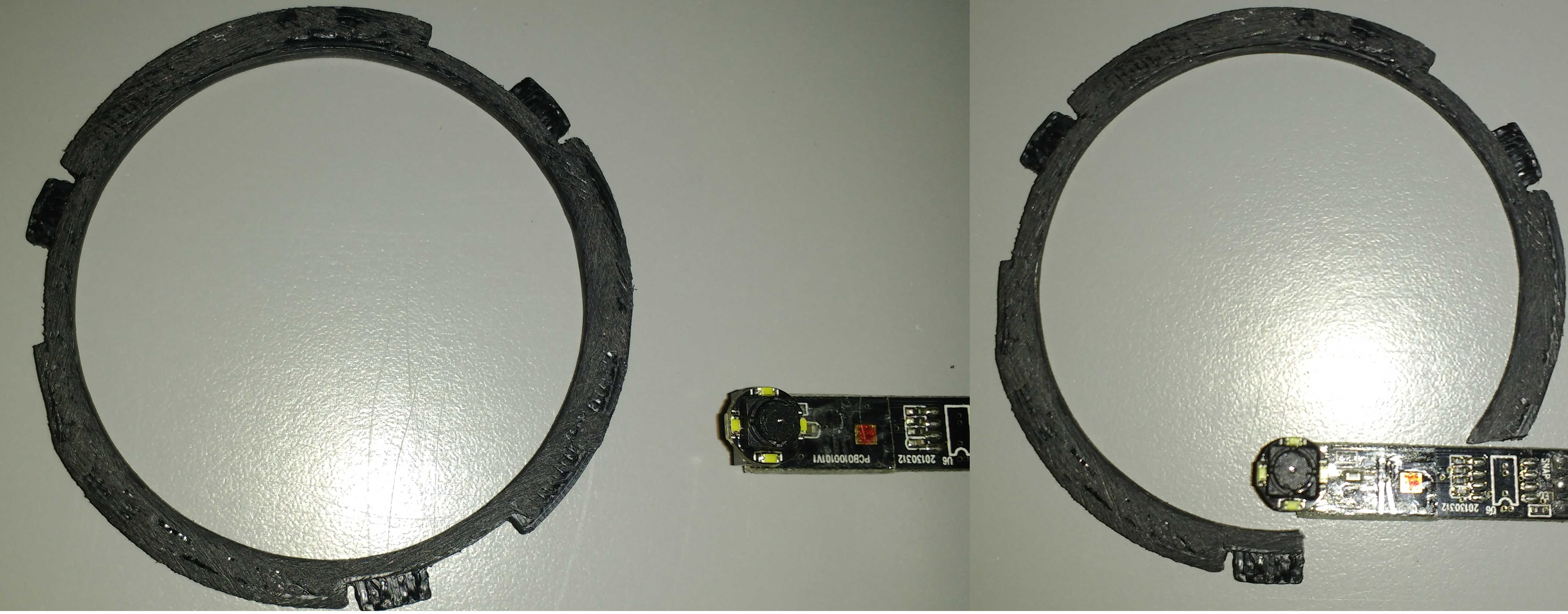
Now we can glue the two pieces together by matching the top and lower parts, as shown below.
Click here to watch the video showing the assembling.
IR LED ring
In order to provide a shadow free illumination to the user's eyes, 8 IR LEDs where placed equidistantly from each order on a circular PCB. In order to meet the safety requirements of using IR illumination some calculations needed to be made. After some experimentation it was decided to power the LEDs with a current of 15 mA. Which for the Vishay VSMY1850ITX01 LEDs means they will produce a radiant intensity of about Ie = 1.5 mW/sr. This will be rounded up to 2 mW/sr, because given the safety concerns discussed previously is best to consider a worst case scenario. The distance from them to the pupil is greater than 2 cm, so the irradiance, for each LED, is about E = I_e/d^2 = 0.5 mW/cm^2. Since the LEDs are very close to each other the sum of their average irradiance must be taken into account. For each ring this gives E_total = 8.E_IR = 4 mW/cm^2, which is less than the 10 mW/cm^2 recommendation, for periods of over 1000s. If we consider the contribution of both illumination rings the total irradiance is still under this limits. It's important to note that these calculations assume a constant radiant intensity independent of the angle between the LEDs and the pupil. As with most LEDs the radiant intensity decreases as the angular displacement increases. For instance, at 30º the radiant intensity decreases by 10% and at 40º by 20%. As the pupil is at an angle between 30 or 40º, in relation to the LEDs, the real world values are less than those calculated.
Supplied with 15mA the forward voltage of each LED is about 1.4V, so the circuit in figure below was designed to powered them.
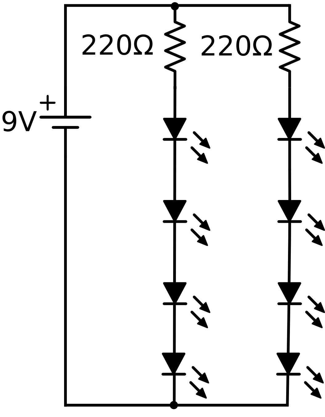
On the next figure, a suggestion of the PCB circuit is presented. This design was chosen so as to simplify the manufacture process. Where "V+" and "V-" represent, respectively, the positive and negative voltage terminals, and "R" represents the resistors.
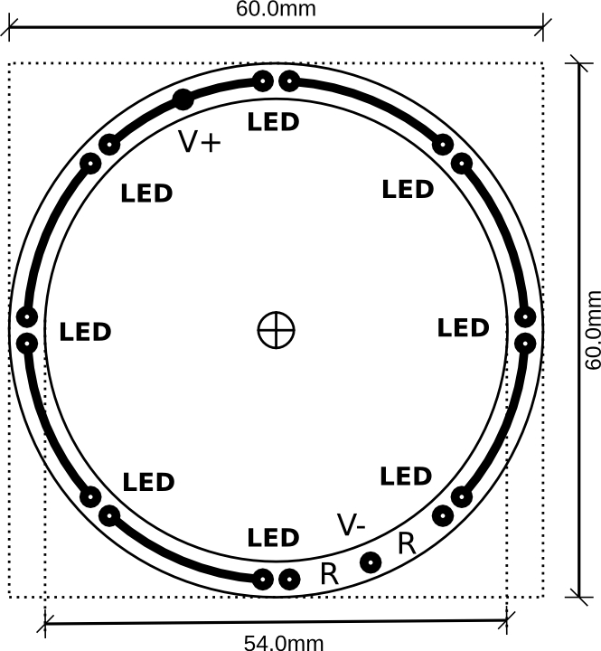
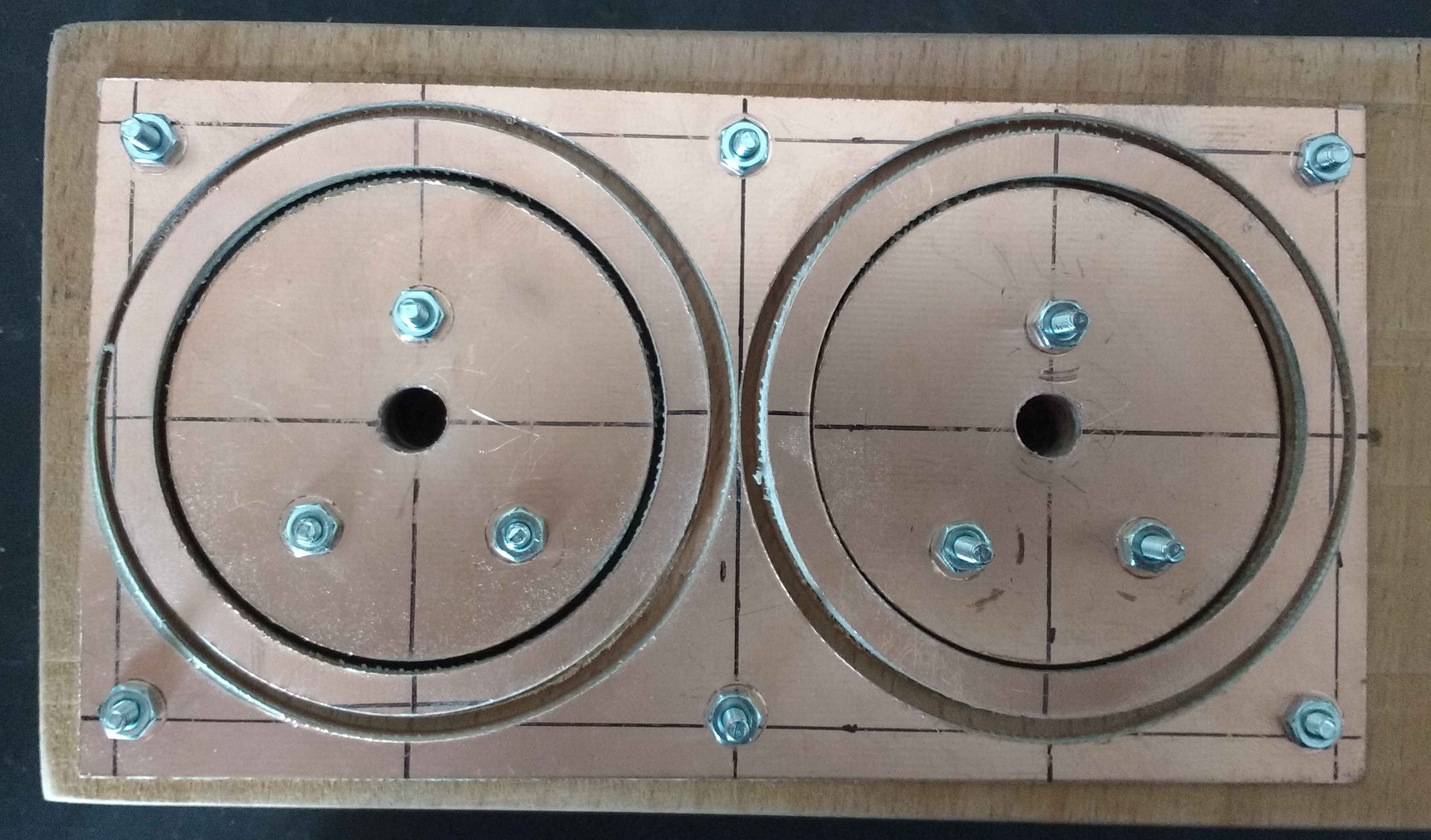
Due to their circular, and hollow shape (which leads to a high loss of material), the commercial \ac{PCB} manufacturers we've contacted, placed a considerable high price on their manufacture (upwards of 30€ per eye, without components). Considering the low cost of raw PCB, and the simplicity of the circuit, a cheaper alternative is to do it in house. Locally, in Portugal, the PCB cost per cm^2 is between 1 or 2 cents, depending on the size of the board. The rings have a diameter of 6 cm, so their cost will be far less than 1€ per ring. The figure below shows the jig used to hold the PCB in place,
while the cuts where made using different sized hole saws. Note that for the inside cut of the rings, the hole saw must be chosen measuring it's outside diameter, and for the outside cut the opposite applies. If they are not available a coping saw or a jigsaw could be used, to give some alternatives.
Since the PCB layout consists of simple interruptions of the copper layer, etching can be replaced with the use of a blade or file to remove the material. The following image shows the finished rings with the components soldered.
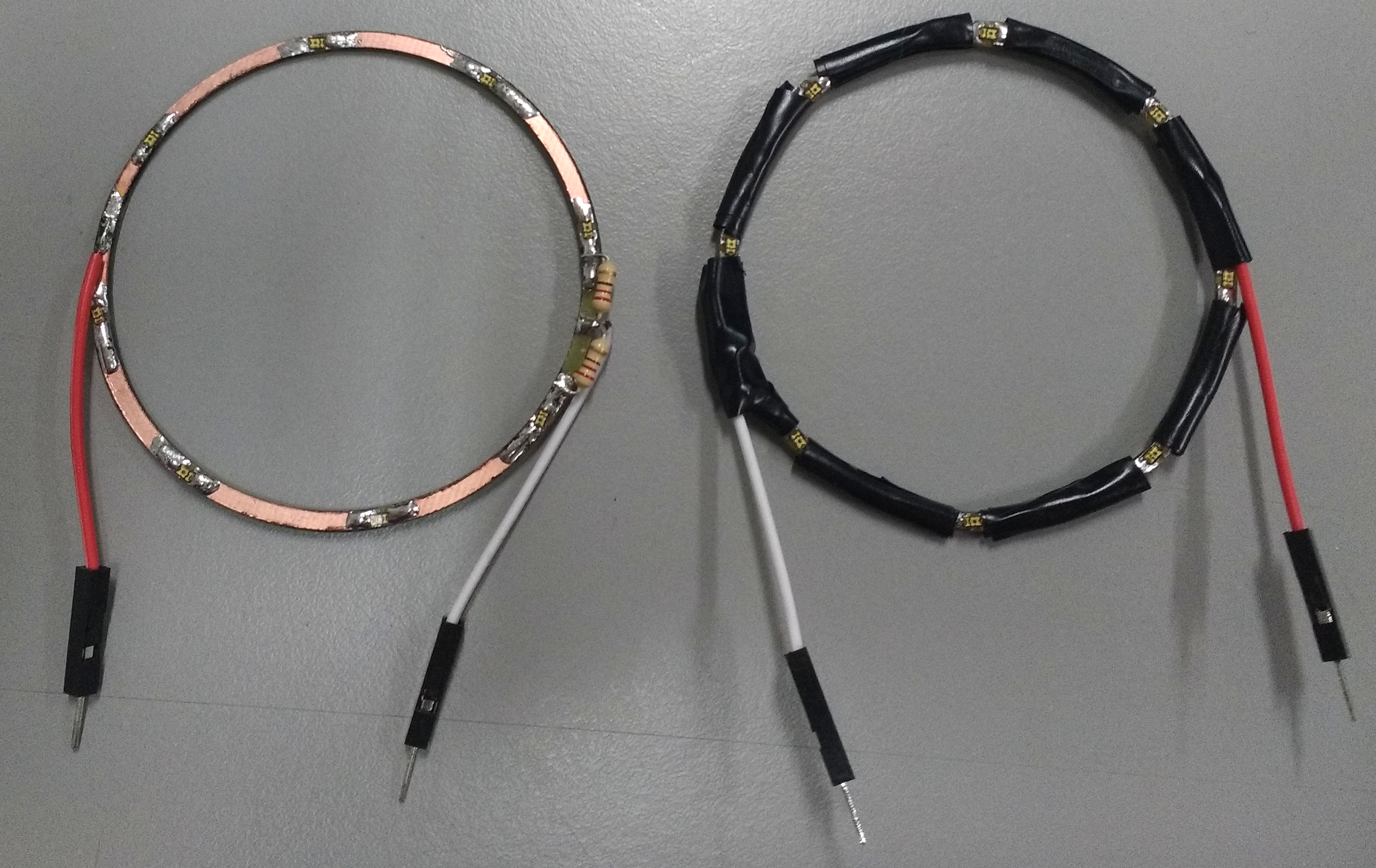
Their total cost was about 20€, of which 8€ was the shipping cost of the LEDs.
Examples of use